
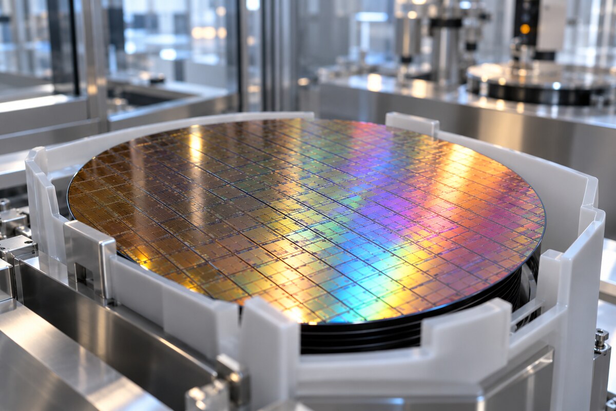
ASML and Belgian semiconductor research organisation imec opened their High NA EUV test laboratory in Veldhoven, in the Netherlands, on Jun 3, 2024. Chip manufacturers, equipment suppliers and materials companies gained early access to a new generation of lithography equipment. Reuters put the first-of-its-kind tool’s value at €350 million, approximately $380 million. The shared facility followed several years of development.
A scanner surrounded by a process laboratory
The joint facility combines the prototype TWINSCAN EXE:5000 with equipment for preparing, processing and measuring wafers. Its infrastructure includes a coating and development track, metrology instruments, and systems for handling wafers and masks. Logic and memory manufacturers can develop private applications before their own factories have operational High NA scanners. Materials and equipment suppliers also have access, alongside imec’s patterning programme.

Preparations began in 2018. ASML and ZEISS worked on the source, optical system, unequal image reduction, field stitching, depth of focus, edge placement and overlay accuracy. Imec and its suppliers prepared resists, underlying films, masks, inspection methods, optical proximity correction and etching. Early exposures produced 10 nm-wide dense lines at 20 nm pitch in metal-oxide resist.
Imec president and CEO Luc Van den hove envisaged the Veldhoven laboratory as an extension of the organisation’s 300 mm cleanroom in Leuven, Belgium. At opening, the partners anticipated manufacturing adoption in 2025–2026. That was their stated timetable; the subsequent experiments below retain their actual dates.
Different optics, smaller exposure fields
The EXE platform increases numerical aperture from the NXE platform’s 0.33 to 0.55, while retaining the 13.5 nm wavelength of extreme ultraviolet light. Numerical aperture describes an optical system’s ability to collect and focus light. Larger mirrors provide the higher aperture, but also change the angle at which light reaches the patterned reticle. An excessive angle reduces the reticle’s reflectivity. Anamorphic optics address that problem with different reduction factors: four in one direction and eight in the other. Standard-sized reticles remain usable. The exposed field, however, is half the size of an NXE field, requiring twice as many exposures per wafer.

Faster moving stages compensate for the smaller field. On Jan 25, 2024, ASML specified wafer-stage acceleration of 8g and reticle-stage acceleration of 32g. The company rated throughput at more than 185 wafers per hour for the EXE:5000, with 220 targeted for 2025. The platform also retains modular construction: individual modules can be tested before assembly into the complete scanner.
Building and measuring the mirrors
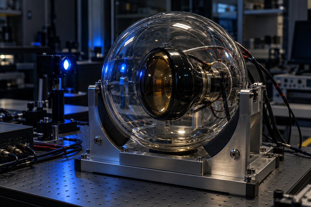
ZEISS manufactures the optical system. Its projection optics weigh approximately twelve tons and contain more than 40,000 components, in specifications published on Jan 30, 2024 and updated on Jan 21, 2025. The illumination system has approximately 25,000 parts and weighs more than six tons. These are separate assemblies within the lithography system. The mirror surfaces carry more than 100 extremely thin silicon and molybdenum layers. Each deposited layer is only a few atomic layers thick. Peter Kürz, who headed ZEISS SMT’s High-NA-EUV business field, described the larger mirrors as a means of collecting more light and directing it with greater precision.
Mirror verification required a separate development programme with ASML. A measuring machine weighing 150 tons checks the optics inside vacuum chambers approximately five metres in diameter. That weight belongs to the metrology apparatus, rather than the wafer scanner. ZEISS put its High NA research effort at approximately ten million working hours, with more than 2,000 patents and around 1,200 network partners contributing to the technology’s development.

Preparing materials and joining exposure fields
Before the laboratory opened, imec prepared processes for transfer to the prototype. Its Feb 26, 2024 programme included field stitching: joining patterns across the smaller exposure fields created by anamorphic optics. The preparatory stitching work used an NXE:3400C scanner, with ASML and mask-making partners. It was distinct from later experiments on the High NA machine itself. Metal-oxide resists led the programme for line-and-space patterns. Selecting underlayers and adjusting development, mask absorbers, mask bias and mask tonality reduced exposure dose by more than 20% without increasing roughness or stochastic failures in those experiments. Tip-to-tip dimensions were preserved.
A separate comparison paired metal-oxide resist with a bright-field mask for contact holes. Against positive-tone chemically amplified resist and a dark-field mask transferred into the same stack, dose fell 6% and local critical-dimension uniformity improved 30%. Mask quality and defects remained concerns. Imec also prepared electron-beam and deep-ultraviolet inspection methods, including proposals to denoise scanning-electron-microscope images with machine learning to help find and classify small defects.
Installing a customer system in Oregon
Intel completed assembly of its EXE:5000 at the D1X research and development site in Hillsboro, Oregon, and began calibration in April 2024. The installation was a separate customer system from the shared Veldhoven laboratory. Intel was preparing the new tool for its future process roadmap when it announced the completed assembly on Apr 18, 2024. Transport involved more than 250 crates packed into 43 freight containers. Cargo aircraft carried them to Seattle, followed by twenty trucks for the journey to Oregon. Intel had opened D1X’s Mod 3 expansion in 2022, investing more than $3 billion and adding 270,000 square feet of cleanroom space to accommodate a new generation of equipment.

Intel planned to combine 0.33 NA and 0.55 NA EUV with other lithography processes. Its announced sequence included product proof points on Intel 18A in 2025 and subsequent Intel 14A production. Those were plans at the time of installation. Intel also intended to acquire the next-generation EXE:5200B, then described as offering productivity above 200 wafers per hour.
Aug 7, 2024: logic and memory patterns
The Veldhoven laboratory’s later tests extended beyond regular arrays of parallel lines. On Aug 7, 2024, imec presented random logic patterns with dense metal lines measuring 9.5 nm across, corresponding to 19 nm pitch. Tip-to-tip dimensions were below 20 nm. The structures were made with a single High NA exposure. Other patterns addressed different layout requirements:
- Random vias had 30 nm centre-to-centre spacing.
- Two-dimensional features reached 22 nm pitch.
- A DRAM-specific layout at 32 nm pitch integrated storage-node landing pads with bit-line periphery structures.
Before exposure, imec prepared wafer stacks with advanced resists and underlayers, along with photomasks. Baseline processes transferred to the scanner included optical proximity correction, integrated patterning and etching. Customers could develop applications using their own design rules and layouts. Steven Scheer, then senior vice president for compute technologies and systems, regarded the results as an initial validation of logic and memory applications. Further maturation of materials and equipment remained part of the partner programme. The demonstrations concerned patterned structures, rather than complete commercial processors.

Feb 24, 2025: electrical testing
Metallised structures subsequently provided a way to examine electrical behaviour. On Feb 24, 2025, imec demonstrated 20 nm-pitch metal lines patterned with a single High NA exposure using a negative-tone metal-oxide resist. Two types of test vehicle—serpentine structures and fork-fork structures—achieved electrical yield above 90%. Serpentine, or meander, structures help reveal breaks in conducting paths. Fork-fork structures expose unwanted bridges. Conductivity measurements, combined with electron-beam inspection, provide information about stochastic defects that reduce yield. Advanced-patterning director Philippe Leray identified resist optimisation for lower dose at a given yield, with minimal additional stochastic failures, as an ongoing effort with resist suppliers.
Imec illustrated the work with top-down electron-microscope images after pattern transfer into a titanium-nitride hard mask and transmission-electron-microscope images of metallised wires after chemical mechanical polishing. The work was prepared for SPIE Advanced Lithography + Patterning. Its yield figure applies to those test structures and processing conditions. It is a different measurement from optical resolution, and does not provide a production yield for a finished chip.
Sep 22, 2025: two metallisation routes
By Sep 22, 2025, imec had demonstrated 20 nm-pitch lines with 13 nm tip-to-tip dimensions relevant to damascene metallisation. Local critical-dimension uniformity reached as low as 3 nm for those tip-to-tip structures. The process combined metal-oxide resist with jointly optimised underlayers, illumination pupil shape and masks. Interruptions in metal tracks require close control of the gaps between line ends. Imec was continuing work on smaller gaps, including promising 11 nm results, and on transferring the structures into an underlying hard mask for damascene interconnects. Those development steps remained ongoing.

A second route used direct metal etching of ruthenium. Single-exposure High NA patterning produced ruthenium lines at 20 nm and 18 nm pitch, including 15 nm tip-to-tip structures and functional interconnects with low resistance. Electrical test yield reached 100% for the 20 nm-pitch metallised line structures. The figure belongs to that particular demonstration, rather than all devices or both pitches. The EU NanoIC pilot line partly enabled the work, presented at the SPIE Photomask Technology + EUV Lithography Conference.
Optical resolution and patterned-wafer performance
High NA’s smallest optical dimensions remain distinct from a complete patterning process. In a Feb 26, 2026 technical review, imec’s Geert Vandenberghe described the scanner’s potential to resolve 16 nm-pitch lines, or 8 nm critical dimensions. Imec had obtained 16 nm-pitch line-and-space images in metal-oxide resist in 2024. Contact holes in chemically amplified resist and pillars in metal-oxide resist reached 24 nm centre-to-centre spacing. The aerial image must then become a developed resist pattern and survive etching into underlying layers. Resists, underlayers, hard masks and etching determine the resulting structures and their yield across a 300 mm wafer. Vandenberghe therefore placed the limit for yielding, industry-relevant patterns above the optical minimum.
Higher image contrast also changes process conditions. Experiments on 29 nm-pitch hexagonal holes and pillars produced local uniformity improvements of 18–42% relative to 0.33 NA features, alongside approximately 60% dose-to-size gains. These comparisons concerned specified patterns. Remaining research included depth of focus, stochastic-defect mitigation and field stitching. Imec also demonstrated bidirectional routing with two-dimensional Manhattan designs at 22 nm and 28 nm pitch. Mask quality and optical proximity correction preserved pattern fidelity after etching.

Sep 8, 2026: extending established resists
Chemically amplified resists, or CARs, offered another materials route. Imec and suppliers demonstrated single-exposure High NA line-and-space patterns down to 22 nm pitch, announced on Sep 8, 2026. Meander and forked test structures showed good pattern fidelity at that pitch.
The work included 24 nm-pitch SRAM layouts with 26 nm tip-to-tip dimensions, 24 nm place-and-route structures with 28 nm tip-to-tip dimensions, and random logic vias separated by 28 nm centre to centre. Earlier results at the 2026 International Interconnect Technology Conference involved 28 nm-pitch lines and metallised electrical test structures 1.8 metres long, with promising combined yields.
Patterning-programmes vice president Geert Vandenberghe attributed the progress to joint optimisation of CAR materials and lithography–etch techniques. Imec envisaged CAR use for selected critical layers at A14/A10 technology nodes, including metal-2, vias and metal-to-diffusion connections. Further optimisation targeted yield and tighter pitches. The node labels identify technology roadmaps; they are separate from the measured line pitches, line-end gaps and via spacings in these experiments.

A broader research partnership
ASML and imec signed a five-year strategic agreement on Mar 11, 2025 covering semiconductor research and sustainable innovation. Its scope extends across ASML’s portfolio: 0.55 NA and 0.33 NA EUV, immersion deep-ultraviolet lithography, YieldStar optical metrology, and HMI single-beam and multibeam technologies.
The agreement envisaged installing these systems in imec’s pilot line and incorporating them into NanoIC infrastructure for research beyond the 2 nm node. Research areas also included silicon photonics, memory and advanced packaging. A new element would support ideas within imec’s research programme intended to deliver environmental and societal benefits.
ASML president and CEO Christophe Fouquet described the agreement as a further step in the organisations’ longstanding cooperation. Van den hove emphasised access to advanced patterning and the expansion of pilot-line capabilities. ASML’s investment was complemented by Chips Joint Undertaking and Flemish-government support for NanoIC, and Dutch-government funding through an Important Project of Common European Interest. Making 0.55 NA technology available at imec formed part of the Dutch-funded Next Gen-7A project.

Extending the infrastructure to Leuven
The first module of a High NA EUV machine reached imec’s 300 mm cleanroom in March 2026. By Apr 2, 2026, the new system was installed within imec’s Leuven research infrastructure. Veldhoven’s joint laboratory had already provided the partners with a place to optimise materials and processing together.
The installation followed a longer EUV history at imec. An early demonstration tool arrived in 2006; industrial-scale EUV chip production followed in 2019. Imec’s technology roadmap extends to 2040, coordinating lithography with new materials, transistor architectures and interconnects. Its research environment brings together chipmakers, equipment and materials suppliers, metrology specialists and designers to refine processes and design rules.
The NanoIC expansion involves installing more than a hundred semiconductor tools. Start-ups, universities and other innovative companies are intended users of the pilot line, alongside the established semiconductor ecosystem. The pilot line provides access for testing ideas and developing applications. Its additional equipment is part of the infrastructure expansion under the EU Chips Act.

















Leave a comment